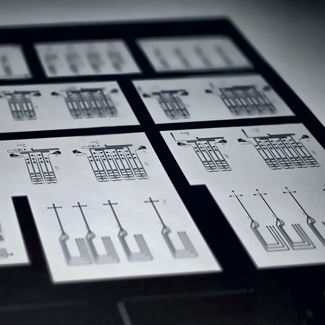
Film Photomask

Film photomasks provide a flexible, high-resolution alternative to glass-based masks for photolithographic applications where rigid substrates are not required.

Product in details

Film Photomask Manufacturing

For applications where the dimensional stability of glass is not a process requirement, Selba’s film photomasks offer a compelling combination of pattern accuracy, format flexibility, and production economics that glass cannot match on cost or turnaround. Produced at up to 50,800 dpi, film photomasks deliver sharp edge definition and consistent feature geometry across a broad range of applications — from PCB conductor patterns and microfluidic channel artwork to encoder graduations and custom optical apertures. Turnaround is fast: orders cleared through Selba’s pre-production file review are shipped within 24 hours of confirmation, allowing artwork revisions to be validated and iterated within a single working day — a critical advantage at the prototyping and development stage where frequent design changes and tight schedules make glass mask lead times impractical. Film substrates are supplied in a wide range of formats, cut to the customer’s required dimensions or produced in specific aspect ratios to match the exposure tool working area, offering format flexibility that rigid glass substrates cannot provide. For customers managing development budgets across multi-stage programmes, film photomasks allow prototyping and early validation to be conducted at a fraction of glass mask cost — preserving budget for the production stage where glass is required. As with all Selba orders, submitted artwork is reviewed by the R&D team before production begins, ensuring that resolution limits and process constraints are resolved before the first film is run.

Motion Feedback

Product Description

Film photomasks provide a flexible, high-resolution alternative to glass-based masks for photolithographic applications where rigid substrates are not required. Produced using the same high-resolution laser photoplotting process as Selba’s glass photomasks, film masks deliver sharp pattern definition and accurate feature reproduction at shorter lead times and lower cost — making them the practical choice for a broad range of industrial lithography, prototyping, and mid-volume production workflows.
Selba’s film photomask service covers applications across printed circuit board manufacturing, photochemical machining, encoder disc production, and industrial patterning processes where film’s handling flexibility and format adaptability are process advantages.
  • PCB & Electronic Fabrication
  • Photochemical Machining
  • Microfluidics & Biomedical Devices
  • R&D, Prototyping & Academic Research
Selba: Film Photomasks and the Economics of Iteration

PRODUCT SPECIFICATIONS

Technical Details

High-Resolution Laser Photoplotting on Film Substrates.

Film photomasks are produced using Selba’s laser photoplotting capability, operating at up to 50,800 dpi, ensuring sharp edge definition and consistent pattern accuracy across the full film area. This resolution level supports fine-feature geometries suited to PCB conductor patterns, etching artwork, and custom graduation patterns, with positional accuracy maintained across the full working format.
Film substrates offer practical advantages over glass in applications where cutting to a specific format, rolling, or handling flexibility is operationally relevant. They are particularly well suited to photochemical machining workflows, where the mask must conform to non-planar or large-format workpieces, and to prototyping environments where rapid design iteration takes priority. Standard input formats including Gerber and DXF are accepted directly, and orders that clear the pre-production file review are shipped within 24 hours of confirmation — one of the shortest lead times available in precision photomask supply.

High-resolution laser photoplotting

Up to 50’800 dpi


Fast shipment after artwork approval

24-hour turnaround

Direct file compatibility

Gerber & DXF formats

Custom dimensions, no standard limits

Flexible format sizing

Sharp contrast and edge definition

High optical density emulsion

Design–produce–test within 24h

Single-day iteration cycle

PRODUCT SPECIFICATIONS

Custom Services

Fast Turnaround Without Compromising Process Integrity.

Every film photomask order begins with a structured review of the submitted artwork by Selba’s R&D experts. Feature geometries, line widths, and critical dimensions are assessed against the intended photolithographic process before production is initiated — ensuring that resolution limits, emulsion characteristics, and format constraints are accounted for before the first film is run. This upstream review is a standard part of the Selba service and is what underpins the reliability of the 24-hour shipment commitment for cleared orders.
For customers at the prototyping stage, the combination of fast turnaround and direct engineering access allows rapid design iteration — artwork can be revised, reviewed, and reproduced in a single working day. For small series and volume programmes, consistent process parameters and inspection protocols across batches ensure that film masks produced in successive runs perform identically within the customer’s exposure process. Selba supports customers from initial artwork preparation through substrate selection, format specification, and process integration, providing a technically grounded supply relationship rather than a transactional one.

Cleanroom Production
Quality Control Process
Certification Standards

CUSTOM & MASS PRODUCTION

Industrial Applications

Technical Details
Film photomasks are the natural choice for the early stages of any photolithographic development programme, where the priority is speed of iteration rather than the dimensional stability and durability that production-stage processes demand. At the prototyping and R&D phase — when device architectures are being validated, process parameters are being optimised, and design geometry is subject to frequent revision — the ability to move rapidly from artwork to exposed substrate is often more valuable than any other single capability a photomask supplier can offer. Selba’s film photomask service is structured around exactly this requirement: submitted artwork files are reviewed by Selba’s R&D team before production, verified against resolution limits and process constraints, and cleared masks are shipped within 24 hours of order confirmation — compressing the design-expose-evaluate cycle to a single working day and allowing multiple design iterations to be tested within a single development sprint. Standard input formats including Gerber and DXF are accepted directly, minimising file preparation overhead between design tool and production. For doctoral researchers, R&D laboratories, and engineering teams developing new device concepts across disciplines including microfluidics, photonics, MEMS, and bioelectronics, Selba’s film photomask service provides the responsive, technically supported production capability that academic and industrial research programmes require — combining the process expertise of a precision optical manufacturer with the turnaround speed and cost structure that early-stage development budgets demand.
Industrial Applications
Selba’s film photomasks are produced on high-resolution photographic film substrates optimised for laser photoplotting at up to 50,800 dpi, delivering the fine-feature resolution, edge definition, and optical density required for demanding photolithographic applications. The film base is a dimensionally stable polyester substrate — selected for its resistance to the humidity and temperature variation encountered in standard handling and storage environments — coated with a high-resolution photographic emulsion that responds to the laser photoplotting process with consistent sensitivity and uniform development characteristics across the full film area. Optical properties are matched to the UV exposure processes the film mask will serve: the developed emulsion provides high optical density in opaque regions and full transmission in clear areas, delivering the contrast ratio required for reliable photoresist exposure with well-defined feature edges and minimal light scatter at pattern boundaries. Film photomasks are supplied in a wide range of format sizes — cut to the customer’s specified dimensions to match the working area of the exposure tool, the substrate format of the process, or the mechanical constraints of the contact or proximity aligner in use. There are no fixed format increments: length, width, and aspect ratio are defined entirely to customer requirement, making film a particularly practical substrate for large-format applications where glass would impose size or weight constraints. Film thickness is selected to match the flatness and handling requirements of the exposure setup, with thicker film bases providing greater dimensional rigidity for precision contact lithography applications and thinner bases offering greater flexibility for processes requiring the film to conform to non-planar or large-area substrates.
Custom Services
Film vs. Glass Photomasks: Choosing the Right Solution
The choice between film and glass photomasks is fundamentally a question of matching the mask specification to the precision, durability, and economic requirements of the application — and understanding where the performance trade-offs between the two become relevant. On cost, film photomasks are substantially less expensive than glass equivalents, making them the practical choice for prototyping, R&D, and any application where frequent design iteration or large-format artwork makes the recurring cost of glass masks prohibitive. On turnaround, film’s advantage is equally clear: Selba ships film photomasks within 24 hours of artwork approval, while glass photomask production involves additional process steps — substrate preparation, chromium deposition, and post-patterning inspection — that extend lead times accordingly. On precision, glass holds the decisive advantage: the dimensional stability of glass substrates under thermal and humidity variation preserves pattern placement accuracy and graduation pitch in ways that polyester film cannot match, making glass the required choice wherever overlay accuracy, feature placement repeatability, or long-term pattern stability are process requirements. On durability, chromium-on-glass photomasks withstand repeated exposure cycles, chemical handling, and mechanical contact without pattern degradation, while film emulsions are more susceptible to surface damage, scratching, and dimensional drift over time — limiting film to applications where the mask is used for a defined number of exposures rather than as a long-term production tool. In practice, the two formats are complementary rather than competitive: film photomasks serve the prototyping, development, and validation phases of a programme, where speed and cost take priority, while glass photomasks serve the production phase, where precision, repeatability, and durability are non-negotiable. Selba produces both, allowing customers to transition seamlessly between the two as their programme matures — with the same R&D-led file review and engineering support applied at every stage.

Use Case

Supporting Doctoral Research Across Multiple Disciplines — A Leading European Research Institute

“Providing film photomask production support to doctoral researchers working across a broad spectrum of advanced scientific disciplines for a prominent European research institute.”

FAQ

Frequently asked questions

What is a film photomask?
A film photomask is a photolithographic patterning tool produced on a flexible polyester film substrate coated with a high-resolution photographic emulsion, rather than on a rigid glass plate. Like a glass photomask, it carries a precisely defined pattern of opaque and transparent regions that modulates UV light during photoresist exposure — transferring the pattern geometry from the mask onto the substrate below. Film photomasks are produced by laser photoplotting, a process in which a precision laser writes the pattern directly onto the photosensitive emulsion at high resolution, developing it into a stable, high-contrast image. The resulting mask is used in contact, proximity, or large-area exposure processes to define conductor patterns, microfluidic channels, encoder graduations, etch masks, and a broad range of other photolithographic features. Film photomasks offer a cost-effective and fast-turnaround alternative to glass for applications where the dimensional stability and durability of a rigid glass substrate are not process requirements.
When should I use a film photomask instead of glass?
Film photomasks are the appropriate choice when speed, cost, and format flexibility take priority over the dimensional stability and durability that glass provides. At the prototyping and development stage — where designs are subject to frequent revision and the priority is rapid iteration rather than long-term mask life — film’s 24-hour turnaround and substantially lower cost per mask make it the practical default. Film is also well suited to large-format applications where glass substrates would impose size, weight, or cost constraints impractical for the process in question, and to applications where the mask is used for a limited number of exposures rather than as a recurring production tool. Glass photomasks become the required choice when pattern placement accuracy across temperature and humidity variation is critical, when the mask must withstand repeated exposure cycles without degradation, or when the lithographic process requires the flatness, UV transmission, and dimensional stability that only a rigid glass or quartz substrate can provide. In practice, many development programmes use film photomasks through prototyping and validation, then transition to glass for production — a workflow that Selba supports at both stages with the same pre-production file review and engineering engagement.
What is photoplotting?
Photoplotting is the process by which a precision laser writes a defined artwork pattern directly onto a photosensitive substrate — film or glass — by selectively exposing the photosensitive coating according to the digital artwork file provided by the customer. In laser photoplotting, the artwork data — typically supplied in Gerber or DXF format — is converted into a raster or vector exposure map that drives the laser across the substrate surface, switching on and off to expose the emulsion or resist in the precise pattern defined by the artwork. The exposed substrate is then developed to produce the finished photomask, with opaque regions defined by the developed emulsion or chromium layer and transparent regions left clear. The resolution of the photoplotting process — expressed in dots per inch (dpi) — determines the minimum feature size and edge acuity achievable on the finished mask. Selba’s laser photoplotting service operates at up to 50,800 dpi, enabling the definition of fine-feature patterns on both film and glass substrates with the edge definition and dimensional accuracy required for demanding photolithographic applications.
What is the accuracy of film photomasks?
The accuracy of a film photomask is determined by two factors: the resolution and positional accuracy of the laser photoplotting process that produces it, and the dimensional stability of the film substrate under the temperature and humidity conditions of use. Selba’s laser photoplotting process operates at up to 50,800 dpi, enabling fine-feature definition with consistent line widths and sharp edge profiles across the full film area. At this resolution, film photomasks are capable of supporting the feature sizes and pattern geometries required across a broad range of industrial photolithographic applications — including PCB conductor patterns, microfluidic channel networks, encoder graduation patterns, and MEMS structural geometries. The principal accuracy limitation of film relative to glass is dimensional stability: polyester film substrates are subject to small but measurable dimensional changes in response to temperature and humidity variation, which can introduce pattern placement error and pitch drift in processes requiring precise overlay or tight feature placement tolerances across the full mask area. For applications where these effects fall within the process tolerance budget, film photomasks provide fully adequate accuracy at substantially lower cost than glass. Where they do not, glass is the appropriate substrate.
Are film photomasks suitable for prototyping?
Film photomasks are ideally suited to prototyping and represent the most practical and cost-effective photomask solution for the development phase of any photolithographic programme. The combination of fast turnaround — Selba ships film photomasks within 24 hours of artwork approval — low cost per mask, and wide format flexibility allows development teams to iterate rapidly through design revisions, process parameter variations, and feature geometry evaluations without the lead time and cost burden that glass photomask production would impose at this stage. Selba’s pre-production file review, carried out by the R&D team before every order enters production, adds a layer of process engineering support that is particularly valuable in a prototyping context: design features that approach resolution limits, artwork geometries that may not transfer cleanly under the customer’s exposure conditions, and format or emulsion compatibility issues are identified and resolved before the film is produced — avoiding wasted experimental cycles. For research laboratories, doctoral programmes, and engineering teams developing new device concepts across microfluidics, photonics, MEMS, bioelectronics, and precision optics, Selba’s film photomask service provides the responsive, technically supported rapid prototyping capability that early-stage development demands.