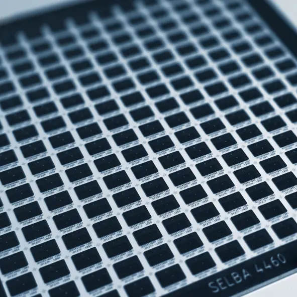
Glass Photomask

Glass photomasks are the master optical tools at the heart of photolithographic fabrication processes, defining precise patterns for semiconductor and electronics manufacturing.

Product in details

Glass Photomask Manufacturing

Glass photomask manufacturing sits at the heart of Selba’s technical identity — the discipline around which its photolithographic expertise and process infrastructure have been built over more than seven decades. Every mask is produced using high-resolution laser photoplotting at up to 50,800 dpi, enabling micron-scale feature definition in chromium or antireflective chromium with consistent line widths, sharp edges, and high optical contrast between opaque and transparent regions — the contrast quality that determines how faithfully the mask pattern is transferred into the photoresist during UV exposure. Substrate selection matches the exposure process: sodalime glass for standard UV lithography, quartz (fused silica) for deep-UV applications requiring superior transmission and dimensional stability across the full exposure field. Inter-feature registration and alignment accuracy are controlled through Selba’s photoplotting process to the micron-level tolerances required by multi-layer lithographic workflows, where successive exposures must align precisely to previously defined structures. Repeatability across production batches is ensured by stable process parameters, consistent substrate and coating materials, and the pre-production file review carried out by Selba’s R&D team before every order enters production — guaranteeing that each mask in a series is dimensionally and optically equivalent to every other, from first article through to volume supply.

Motion Feedback

Product Description

Glass photomasks are the master optical tools at the heart of photolithographic fabrication processes. They define the precise patterns transferred onto substrates during UV exposure — determining the geometry, resolution, and dimensional accuracy of every feature produced in the downstream process. The quality of the photomask directly governs the quality of what is manufactured from it.
Selba produces high-resolution chromium-on-glass photomasks for customers across the semiconductor, electronics, medical device, and optics industries — supplying masks that serve as the critical first link in precision fabrication chains where no error can be introduced at the patterning stage.

  • Semiconductor & Microelectronics Fabrication
  • CNC Machining & Precision Manufacturing
  • Aerospace & Defense Systems
  • Medical Devices & Imaging Systems
Glass Photomask

PRODUCT SPECIFICATIONS

Technical Details

High-Resolution Patterning on Dimensionally Stable Substrates.

Selba’s glass photomasks are produced using high-resolution laser photoplotting, delivering precise feature reproduction and consistent dimensional accuracy across the full mask area. Two substrate materials are offered to match the optical and thermal requirements of the target exposure process. Sodalime glass is suited to standard UV lithography applications, offering a cost-effective and dimensionally stable platform for the majority of industrial photolithographic processes. Quartz (fused silica) substrates are specified for deep-UV applications where sodalime glass exhibits insufficient optical transmission, or where enhanced dimensional stability across the exposure field is required.
Chromium is the standard absorber layer, providing high opacity and sharp, well-defined pattern edges. Antireflective chromium coatings are available for processes sensitive to back-reflection during exposure. Every mask produced at Selba is inspected for pattern fidelity and dimensional accuracy before release, with full traceability maintained from artwork receipt through to final shipment.

Ultra-High Resolution

Up to 50’800 dpi


Thermal Stability Control

≈9 ppm/°C (sodalime) /
≈0.55 ppm/°C (quartz)

Deep-UV Compatibility

Transmission down to 193 nm


Optical Density & Contrast

High-opacity chromium layers


Full Process Traceability

100% inspection
before shipment

Pattern Accuracy & Repeatability

Micron-level tolerances


PRODUCT SPECIFICATIONS

Custom Services

Expert File Review Before Every Production Run.

Selba’s glass photomask service begins upstream of manufacturing. Before any file is committed to production, Selba’s R&D experts review the submitted artwork — assessing feature geometries, critical dimensions, and process compatibility against the intended substrate and exposure process. This review is a standard part of the Selba service, not an optional step, and is what ensures that the delivered mask performs as intended within the customer’s photolithographic process.
Input files are accepted in standard formats including Gerber and DXF. For customers at the prototyping stage, Selba’s integrated facility — combining artwork generation, laser photoplotting, and quality inspection under one roof — enables fast turnaround without subcontractor dependencies. As programmes scale to small series or volume production, the same process parameters and inspection protocols are maintained across batches, providing the consistency that fabrication processes relying on photomask-to-mask repeatability demand. Engineering support is available throughout, including substrate selection guidance, antireflective coating specification, and design-for-process review for customers developing new lithographic workflows.

Cleanroom Production
Quality Control Process
Certification Standards

CUSTOM & MASS PRODUCTION

Industrial Applications

Technical Details
Selba produces glass photomasks on two primary substrate families. Borosilicate glass — including sodalime variants — is the standard choice for UV lithography at i-line (365 nm) and g-line (436 nm) wavelengths, offering good optical transmission, controlled surface flatness, and a thermal expansion coefficient of approximately 9 ppm/°C suited to the majority of industrial and research photolithographic processes. Quartz (fused silica) is specified for deep-UV applications, providing near-complete optical transparency down to 193 nm, a thermal expansion coefficient of approximately 0.55 ppm/°C, and exceptional surface flatness stability across the full exposure field — essential where feature sizes and overlay budgets leave no margin for substrate-induced variation. The absorber layer on both substrates is chromium: standard chromium delivers the opacity and edge definition required for clean pattern transfer across the majority of applications, while antireflective chromium — incorporating a surface oxide layer — suppresses back-reflection at the mask surface, improving image contrast at the resist plane and reducing standing wave effects in processes sensitive to reflected light. Substrate and coating selection is determined in consultation with the customer based on exposure tool configuration and resist process requirements. Surface cleanliness and coating uniformity are verified by inspection before every mask is released, ensuring the photomask arrives at the exposure tool free from defects that could compromise lithographic yield.
Industrial Applications
Glass photomasks are the master patterning tools across every discipline where precise microscale feature definition determines device function and manufacturing yield. In MEMS manufacturing, photomasks define the structural geometries — membranes, cantilevers, cavities, and electrode patterns — that determine the mechanical and electrical performance of sensors, actuators, and microelectromechanical components fabricated by photolithographic etching and deposition processes. In microfluidics, photomasks pattern the channel networks, valve geometries, and reaction chamber layouts of lab-on-chip devices and diagnostic platforms, where the dimensional accuracy of the mask directly governs fluid flow behaviour, mixing efficiency, and assay performance. In semiconductor device fabrication, photomasks define conductor patterns, gate geometries, and interconnect layers across successive lithographic steps, with each mask’s pattern fidelity and overlay accuracy contributing directly to device yield and electrical performance. In biomedical engineering, photomasks support the fabrication of biosensors, implantable microelectrode arrays, and microstructured cell culture substrates, where feature resolution and surface cleanliness determine both device functionality and biocompatibility. In optical systems, photomasks serve as precision reference artifacts and patterning tools for the fabrication of diffractive optical elements, apertures, reticles, and structured illumination components, where the edge definition and optical contrast of the mask pattern determine the quality of the optical function it encodes.
Custom Services
Every glass photomask produced at Selba passes through a structured quality control workflow beginning with a pre-production file review by Selba’s R&D team, who assess submitted artwork for feature geometry, critical dimensions, and process compatibility before any substrate enters production — resolving design issues before they become manufacturing defects. Production is carried out under controlled environmental conditions throughout the patterning, coating, and inspection sequence, with particulate contamination managed at every stage to prevent yield-limiting defects from propagating into the customer’s lithographic process. Dimensional accuracy — covering pattern fidelity, line width consistency, edge definition, feature placement, and coating uniformity — is verified by optical inspection before every mask is released. Full production traceability is maintained from substrate receipt through to final inspection, supporting the qualification and process control requirements of customers in semiconductor fabrication, medical device manufacturing, aerospace, and research environments. As Selba progresses toward ISO 9001 certification by Q1 2027, this inspection and traceability framework is being formalised within a structured quality management system, reinforcing the process discipline that has underpinned Selba’s photomask production for over seven decades.

Use Case

Developing High-Resolution Quartz Photomasks for Deep-UV Semiconductor Lithography

“Implementation of 20um pitch scales for robotic surgical arms, improving positioning repeatability by 15%.”

FAQ

Frequently asked questions

What is a glass photomask?
A glass photomask is a precision optical tool used in photolithographic processes to transfer a defined pattern onto a light-sensitive substrate. It consists of a flat glass plate — borosilicate or quartz — coated with a patterned chromium layer that defines precise opaque and transparent regions. During UV exposure, light passes through the transparent regions to expose the photoresist beneath, while the chromium blocks light elsewhere. The exposed photoresist is then developed and used as a masking layer for etching or deposition. The photomask is the master tool in this process — its dimensional accuracy, feature resolution, and optical quality directly determine the fidelity and yield of every downstream fabrication step performed against it.
What are the advantages of glass photomasks over film photomasks?
Glass photomasks offer decisive performance advantages over film in applications where dimensional stability, feature resolution, and pattern durability are critical. Glass substrates are insensitive to the humidity and temperature variation that cause film to expand, contract, and distort — changes that translate directly into pattern placement error and overlay inaccuracy. Superior surface flatness maintains consistent working distance across the full exposure field, ensuring uniform resolution and exposure dose. Chromium absorber layers provide sharper edge definition, higher optical density, and far greater resistance to mechanical wear than film emulsions, making glass masks suitable for repeated exposure cycles without degradation. Film remains a practical choice for prototyping and large-format applications where glass-grade stability is not required, but wherever resolution, overlay accuracy, and repeatability are paramount, glass photomasks are the unambiguous choice.
What is the resolution of a glass photomask?
The resolution of a glass photomask is determined by the patterning process, substrate, absorber layer, and the optical parameters of the downstream exposure system. Selba produces glass photomasks using high-resolution laser photoplotting at up to 50,800 dpi, enabling micron-scale feature definition with consistent line widths, sharp edges, and accurate placement across the full mask area. This capability supports applications ranging from PCB conductor patterns and MEMS structures to microfluidic channels, encoder graduations, and precision optical components. The practical resolution limit in any given application is also governed by the exposure wavelength, numerical aperture, and photoresist process used downstream — factors assessed by Selba’s R&D team during the pre-production file review to ensure the mask specification is matched to the customer’s exposure process.
What materials are used in glass photomasks?
Glass photomasks comprise two principal materials: the substrate and the absorber layer. Borosilicate glass is the standard substrate for UV lithography at i-line (365 nm) and g-line (436 nm) wavelengths, offering good optical transmission, controlled flatness, and a thermal expansion coefficient of approximately 9 ppm/°C. Quartz (fused silica) is specified for deep-UV applications, providing optical transparency down to 193 nm, a thermal expansion coefficient of approximately 0.55 ppm/°C — fifteen times lower than borosilicate — and superior flatness stability across the exposure field. The absorber layer on both substrates is chromium: standard chromium suits the majority of applications; antireflective chromium — incorporating a surface oxide layer — is specified where back-reflection from the mask surface would otherwise degrade image contrast at the resist plane.
How durable are glass photomasks?
Glass photomasks are significantly more durable than film alternatives, designed to withstand repeated exposure cycles without pattern degradation. The chromium absorber layer resists mechanical wear, chemical exposure, and UV radiation, maintaining optical density and edge definition across extended service lives under normal handling and storage conditions. The glass substrate is dimensionally stable and chemically inert, preserving flatness and pattern placement accuracy over time. Practical durability depends on handling discipline — glass is susceptible to surface scratching and edge chipping if handled carelessly, risks managed through proper storage protocols and protective pellicles in high-volume environments. When handled correctly, a Selba glass photomask maintains its dimensional and optical performance across the full production lifetime of the process it serves — making it a long-term precision asset rather than a consumable component.