
Use Cases



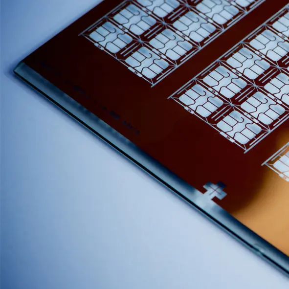
#1 GLASS PHOTOMASKS
Use Case
Read more
Supplying High-Precision Glass Photomasks for Smart Card Chip Fabrication
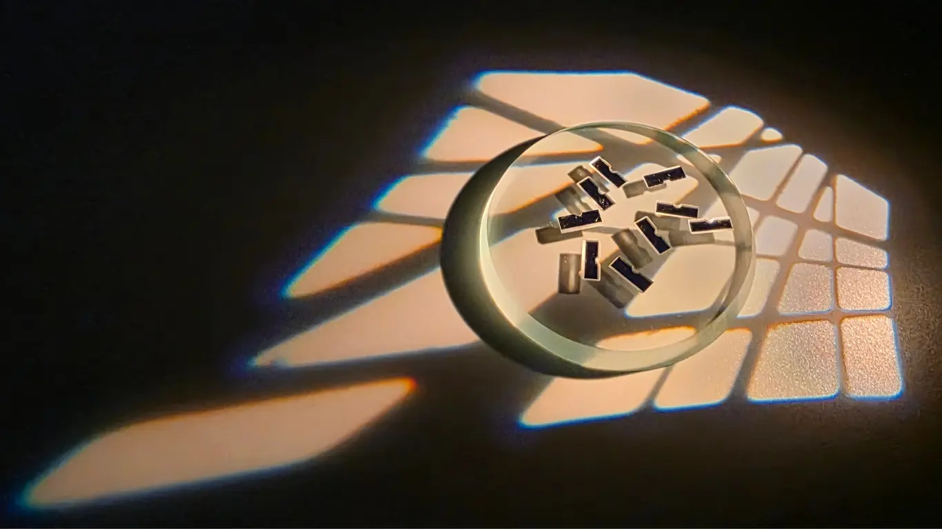
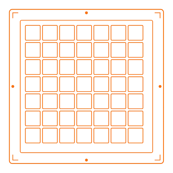
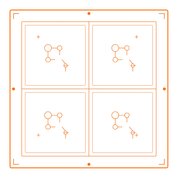
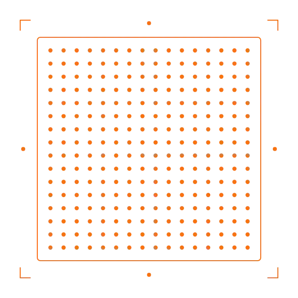
A European smart card chip manufacturer required glass photomasks capable of defining the fine-feature conductor and component geometries central to chip fabrication. The requirements were demanding: the masks needed to deliver Micron pattern accuracy, consistent edge definition across the full exposure field, and dimensional stability sufficient to maintain registration across repeated exposure cycles. Any deviation in the photomask pattern would propagate directly into the manufactured chip geometry — making photomask quality a critical process variable.
Selba’s R&D team reviewed the customer’s artwork files prior to production, verifying critical dimensions and confirming process compatibility with the selected substrate and chromium layer specification. Sodalime glass substrates with a standard chromium absorber layer were selected to match the customer’s UV exposure process, with pattern inspection carried out on each mask prior to shipment to confirm that dimensional accuracy met the tolerances required for reliable chip fabrication.
The collaboration enabled our customer to source a consistent, technically validated photomask supply from a Swiss precision manufacturer aligned with the quality and traceability standards demanded by the microelectronics industry. The partnership reflects the type of long-term, engineering-led supplier relationship that Selba builds with customers operating at the leading edge of European microelectronics manufacturing.

#2 OPTICAL ENCODER DISCS
Use Case
Read more
Developing a 200 mm Glass Encoder Disc for a High-Resolution Rotary Encoder System.
A European manufacturer of precision rotary encoders approached Selba with a requirement that fell outside the capabilities of their existing supply chain: a glass encoder disc with a diameter of 200 mm, combining the optical graduation accuracy of a standard photolithographic process with the mechanical rigidity needed to survive integration into a large-format industrial encoder assembly.
At 200 mm diameter, conventional flat glass substrates of the thickness required for the graduation process presented an unacceptable risk of flexure and fracture during handling, assembly, and operation — compromising both the integrity of the graduation pattern and the long-term reliability of the assembled encoder. Standard edge profiles were insufficient to address the stiffness requirement without increasing substrate thickness to a point that conflicted with the customer’s mechanical envelope.
Selba’s R&D and glass machining teams developed a dedicated machining process incorporating a chamfered edge profile around the full disc perimeter. The chamfer geometry was designed to redistribute mechanical stress at the disc boundary, significantly increasing resistance to flexure and impact without adding substrate mass or altering the optical graduation area. The process required the development of custom tooling parameters within Selba’s in-house glass machining department to maintain precise concentricity between the chamfered profile and the photolithographic pattern — ensuring that mechanical processing introduced no positional error into the graduation.
The resulting disc met the customer’s resolution, signal quality, and dimensional requirements while delivering the structural robustness necessary for reliable operation in an industrial environment. The chamfered glass process developed for this programme has since been integrated into Selba’s standard capability offering for large-format encoder disc applications.
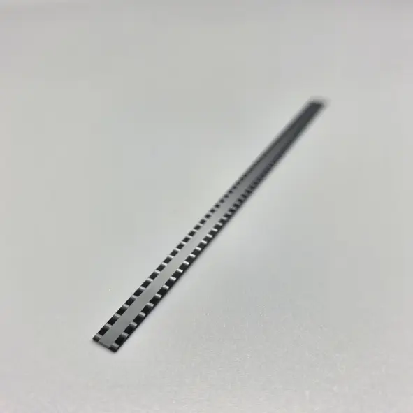
#3 OPTICAL LINEAR SCALES
Use Case
Read more
Selba produced the graduation by laser photoplotting at up to 50,800 dpi, holding pitch and line placement to the micron-level tolerances a 20 µm period demands, verified by optical inspection before release. Black glass was specified as the substrate to absorb stray light and suppress back-reflection from the non-reflective regions, raising contrast at the detector and improving signal quality. The reflective tracks and the absorbing background were patterned in a single process, and the scale was machined to its 40 mm format, with length held to ±0.1 mm and thickness to ±0.05 mm, within the same facility. Keeping the graduation referenced to the finished edges eliminated the tolerance stack-up two separate suppliers would have introduced.
The scale met the manufacturer’s resolution and signal-quality targets at first article. Selba now supplies it as an ongoing production part.
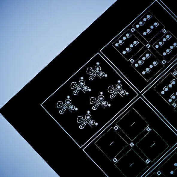
#4 FILM PHOTOMASKS
Use Case
Read more
Supporting Doctoral Research Across Multiple Disciplines — A Leading European Research Institute.
Selba has established a long-running supply relationship with a prominent European research institute, providing film photomask production support to doctoral researchers working across a broad spectrum of advanced scientific disciplines. The collaboration spans multiple research groups and applications — including photonics, microfluidics, bioelectronics, and precision optics — reflecting the versatility of Selba’s film photomask capability and its ability to respond to the highly varied and often rapidly evolving requirements that characterise academic research environments.
Doctoral researchers present a distinctive set of supply challenges. Project timelines are tight, design iterations are frequent, and the range of pattern geometries, feature scales, and substrate formats requested varies significantly from one research group to the next. Standard catalogue products are rarely adequate — each film typically corresponds to a unique experimental design, produced in small quantities and often revised as the research progresses. At the same time, the scientific validity of experimental results depends directly on the accuracy and consistency of the photomasks used to fabricate the test structures and devices under investigation.
Selba’s R&D team reviews every submitted artwork file before production, regardless of volume or application — assessing feature geometries and critical dimensions against the photolithographic process the researcher intends to use. This review has proven particularly valuable in an academic context, where researchers are frequently operating at the limits of their exposure equipment’s capability and benefit from the input of an experienced process engineering team before committing a design to film. In several instances, the pre-production review has identified feature geometries that would not have resolved correctly under the researcher’s exposure conditions, allowing the design to be adjusted before production — avoiding wasted experimental cycles.
Films are produced at up to 50,800 dpi and shipped within 24 hours of artwork approval, a turnaround that accommodates the time-sensitive nature of experimental programmes operating within academic project schedules. The breadth and consistency of Selba’s support across research groups has made it a trusted production partner embedded in the institute’s research workflow — relied upon not only for film supply, but for the process expertise that comes with it.
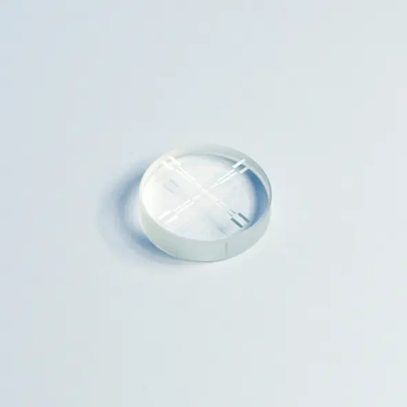
#5 CALIBRATION TARGETS
Use Case
Read more
Supplying Precision Calibration Plates for a Revolutionary CNC Tooling Concept — Swiss Precision Manufacturer.
A Swiss precision engineering company developing a novel CNC machine architecture approached Selba with a calibration plate requirement that no standard supplier could address. The machine’s unconventional design imposed specific and non-standard demands on the calibration artifacts used within its tooling equipment — with pattern geometry, substrate format, and feature placement accuracy defined entirely by the machine architecture. Any deviation in the calibration plate would propagate directly into the machine’s positioning performance.
Selba’s R&D team worked with the customer’s engineers to translate the CNC system’s optical and mechanical specifications into a fully custom calibration plate design, covering pattern layout, feature pitch, substrate material, and external geometry. Artwork was reviewed before production was initiated, and first-article plates were dimensionally inspected against the agreed specification before series supply commenced.
The integration of photolithography and glass machining within a single facility proved critical — the plates required both precise photolithographic patterning and a machined external profile referenced to a specific mechanical datum, a combination that would have introduced unacceptable tolerance stack-up across two separate suppliers. Selba continues to supply calibration plates to the customer as an ongoing production partner, supporting both the development of the CNC platform and its broader commercial deployment.
#6 FINE GLASS MACHINING
Use Case
Read more
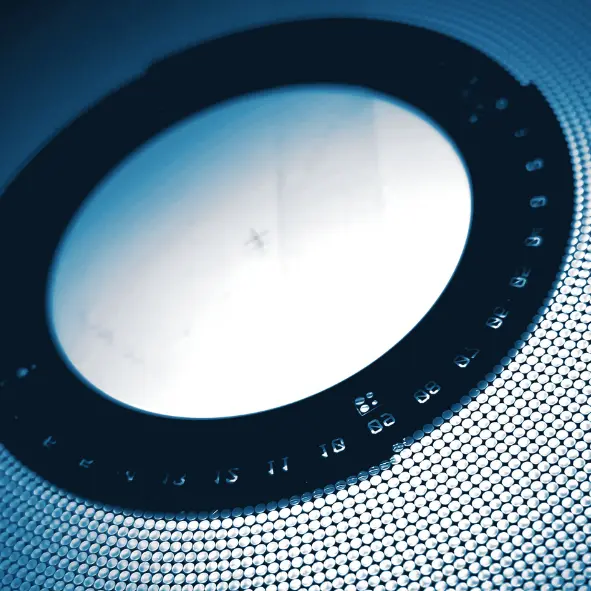
Fast-Turnaround Optical Wafer Machining for a Global Photonics Manufacturer.
A globally active photonics company specialising in high-performance laser and illumination solutions required a machining partner capable of processing optical glass wafers at the turnaround speeds demanded by its production programme. Standard suppliers were unable to meet the combined requirements of geometric precision, edge quality, and delivery speed — wafers needed to be cut and profiled to tight dimensional tolerances while preserving the surface integrity essential for subsequent optical processing steps.
Selba developed dedicated tooling parameters for the customer’s wafer geometry and substrate material, with particular attention to edge condition and surface finish throughout the machining sequence. First-article validation was completed rapidly thanks to Selba’s integrated engineering and production environment. Machined wafers were dimensionally inspected before each shipment, with turnaround consistently meeting the customer’s production schedule.
Selba continues to supply machined wafers to the customer as an ongoing production partner, providing the precision and delivery reliability that photonic component manufacturing demands.